So You Want to Build a Conference Hardware Badge!
Ray Felch //

Recently, it was suggested that it would be cool to create a hardware badge for one of the upcoming InfoSec conferences. Admittedly, I have a pretty solid background in electronic circuit design and software development; however, a conference hardware badge was a relatively new concept to me. Fortunately for me, I have a son that’s been working in the Information Security environment for a number of years and is also an avid collector of conference badges. After checking out some of the badges in his collection and conducting many Google searches, I soon discovered that conference badges can run the gamut from very simple, cool, blinky-light boards to more elaborate, “CTF” hackable, printed circuit boards (PCBs).
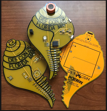
Many of these badges can take on some pretty unique shapes and interesting silkscreen images in their designs. A few months ago, I had the opportunity to connect with Jonathan Singer at the B-Sides conference in Tampa. Jonathan took time out from his schedule to talk to me, and he provided me with an add-on board to his 2018 Unofficial DEFCON 26 badge, which he had designed a few years ago. It’s reassuring to know that he chose the same PCB fabrication house (PCBWay) that I had been working with.
Outline
For this write-up, I have decided to use my first attempt at creating a hardware badge as a process walk-through (as this proved to be a valuable learning experience). I will be highlighting the steps involved in producing the badge from start to finish, including sharing some of the obstacles I needed to overcome. In the process, I will offer some useful tips on electronic circuit design, as well as provide some code development tricks and tools, and helpful information about using the Arduino Uno as a development board.
Moreover, I’ll show the process of how to convert the working electronic breadboard circuit to a PCB using a CAD design system, and ultimately build the PCB using one of the many available fabrication manufacturers. This write-up will show some of the options available and potential problems you might encounter during this phase of the development.
Additionally, we’ll discover some of the options available to us, with regard to building a cost-effective finished product. This might involve outsourcing the CAD design overseas (Pakistan) and fabricating/assembling the PCB in China (PCBWAY, PLCPCB, etc.). These options, while offering lower prices, can introduce long lead-times and can also significantly delay communications between the developer, designer, and manufacturer should questions arise. It wasn’t long before I realized just how many moving parts go into creating the badge from start to finish.
Fun fact: I quickly learned that, in my time-zone, flipping AM to PM (or PM to AM) and adding an hour gets me the time in China (PCBWAY) right now. Likewise, flipping AM to PM (or PM to AM) and subtracting two hours gets me the time in Pakistan (PCB CAD designer) right now.
Electronic Design Phase
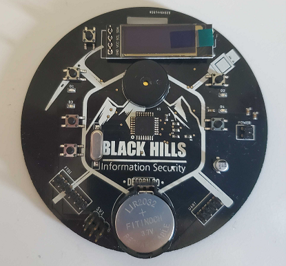
As one might guess, this is my favorite part of the overall process of building a hardware badge. Before getting started, I needed to come up with a theme for the badge that would be entertaining as well as educational. Obviously, the ‘theme’ for a conference badge can vary tremendously, but with this being my first journey into uncharted waters, I decided to keep it relatively simple. For my badge, I chose to model the Milton Bradley (now Hasbro) electronic game, “Simon”, launched in 1978. This popular game generates a sequence of tones and colored lights, which in turn requires the player to repeat the sequence. The sequence grows in size as gameplay continues. As this hardware badge is targeted for an InfoSec audience, I decided to go with the name “CyMon”, as a play on words.
Software Platform
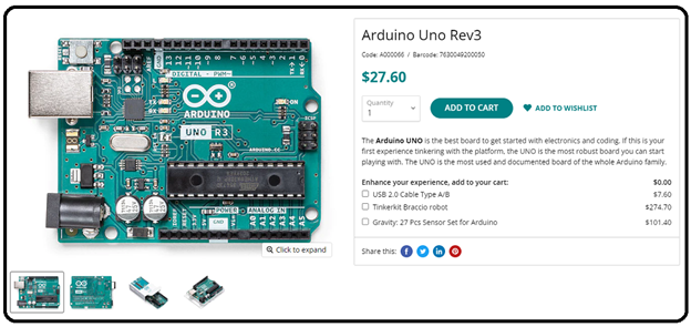
The past couple of years, I have been doing a great deal of software/hardware development using the Arduino IDE and Arduino Uno development board. Other development platforms exist, and I also experimented with Platform IO using Microsoft Visual Studio. At its core, the Arduino Uno development board uses the Atmel ATMega328P microprocessor and is a very cost-effective 16MHz processor, providing 14 digital input/output pins (6 can be PWM outputs) and 6 analog inputs. There is also a great deal of Arduino-based information on the web, and finding Arduino-based examples of the Simon game was fairly easy to locate.
The Arduino IDE has a great, easy-to-use GUI (graphical user interface), making it easy to write code and upload to the board. The specifics on how to get started using the Arduino IDE are beyond the scope of this write-up, but suffice it to say, it should be a fairly short learning curve, especially with all of the help of the Arduino community, forums, bloggers, and support on the web.
Getting Started on the Breadboard
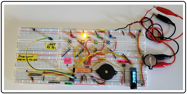
Now that we have the theme for the CyMon badge, we can begin gathering the required components to breadboard the circuit. Again, learning how to breadboard could be a write-up of its own, and this write-up assumes the reader has the basic knowledge of how the breadboard is constructed and how to inter-connect the various components.
Based upon the concept of gameplay of the Simon game, we will need 4 different color LEDs (light emitting diodes): blue, green, red, and yellow. We will also need to limit the current through these LEDs with a 330 ohm resistor, so that they don’t exceed the LED specs and burn out.
Additionally, we will need 4 momentary (normally open) switches to capture the user’s gameplay selections. Typically, one side of the switch will be pulled high (through a 10k resistor) to Vcc (3.3 volts). The opposite side of the switch will be tied to ground (0 volts). When the button is pressed, the switch closes, changing the signal from 3.3 volts (digital 1) to Ground (digital 0). Note: In order to reduce key-bounce (chatter) we will bypass the switches to ground using a 0.1uF ceramic capacitor.
For the audio tones, we’ll need a piezo (speaker), and for communicating with the user, we’ll be using an I2C OLED display. We also will be including 2 more momentary (NO) switches, in addition to the 4 gameplay switches. These two switches will be a reset switch for the processor and a new game (start over) switch, and will require the same 10k resistors and 0.1uF bypass capacitors.
Finally, for the microprocessor circuit, we will need the ATMega328P 28-pin microprocessor, a 16MHz crystal (required for high speed external clocking of the microprocessor), and (2) 22pF bypass capacitors (for clock stability), as well as a toggle (power-on) switch. The breadboard can be powered using a 3.7 volt rechargeable CR2032 button battery, so we’ll need a button cell battery holder and a couple of 10uF electrolytic capacitors for the power rails.
Components
- (4) LEDs blue, green, red and yellow
- (4) 330 ohm resistors
- (6) tactile momentary (NO) switches
- (6) 10k pullup resistors
- (1) Piezo (speaker)
- (1) OLED display
- (1) ATMega328P microprocessor
- (2) 22pF ceramic capacitors
- (1) 16MHz crystal oscillator
- (6) 0.1uF ceramic capacitors
- (1) slider DPST toggle switch
- (1) button cell battery holder
- (2) 10uF Electrolytic capacitors
Looking at the list of components, we should note that most are passive components (typically unaffected by reverse-polarity or voltage issues, etc.). Of the components listed, the microprocessor and OLED display are considered active components. Active components can be severely damaged if wired incorrectly or subjected to high voltage levels that exceed the specified ratings of the device. Likewise, care must be given to the wiring of active components with regard to ensuring Vcc is connected only to the pins marked accordingly. Connecting Vcc directly to a GPIO (general purpose input/output) pin can permanently damage the device. This will become more relevant later in the write-up, when we test our prototype PCBs.
Note: Although resistors, capacitors, and switches are considered passive components and less susceptible to damage, under extreme conditions of high current draw or high voltage levels, any component can be damaged if the circuit is improperly designed. That being said, the circuits described in this write-up are very common configurations that draw very little current and typically operate on 3.3 volts to 5 volts. Obviously, a damaged component at the breadboard stage is going to have less of an impact on the entire build process than would be the case at the prototype testing stage. The former stage simply requires lifting the damaged component from the breadboard and replacing the device, whereas the latter stage requires special surface mount device (SMD) equipment and tools to remove the damaged device. Likewise, applying power to the (latter stage) prototype board without first checking proper orientation of active components can be a major headache (as we will soon see).
How to Get Help With Individual (Sub-Circuit) Component Designs
During the breadboard stage, when designing the hardware badge overall circuit, I found it helpful to do a Google search for ideas on how to implement the various sub-circuits. For example, we could search “Arduino OLED display DIY”, or “Arduino piezo DIY”, or “Arduino momentary switch DIY”, or “Arduino LED DIY”, etc.
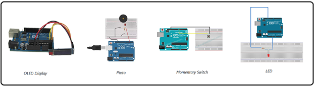
Not only do these search links provide helpful wiring diagrams and great tutorial videos, they typically provide sample sketches (code blocks) that can be uploaded to the Arduino Uno Development board for testing and debugging your code. Once you verify a particular sub-circuit works as you intend it to, you can move the component(s) and its wiring to your main breadboard.
Wiring the ATMega328P 28-pin Microprocessor Dual Inline Package (DIP)
A huge step in designing your own electronic circuitry is to learn the details of your Development board’s microprocessor, and incorporate that microprocessor on your breadboard. Upon close examination of the Arduino Uno’s onboard microprocessor, you will notice it uses a 28-pin DIP package ATMega328P device.
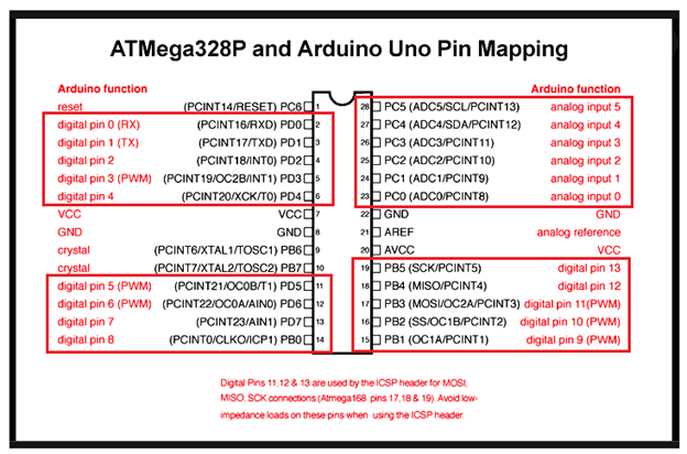
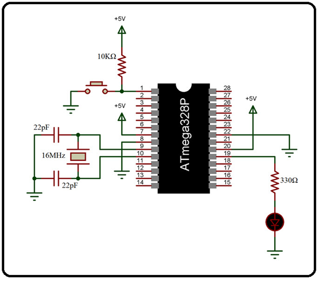
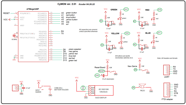
Armed with this knowledge, we can now install the ATMega328P processor on our breadboard and harness much of the capability of the Arduino Uno Development board. The following diagram shows the pin-by-pin wiring of the ATMega328P and its corresponding handful of components (16MHz crystal, 2 – 22pF capacitors, reset momentary switch and 10k resistor). Also shown in this diagram is an LED and corresponding 330 ohm current limiting resistor (as an example). Comparing the two diagrams, we can see that the LED is tied to pin 19 of the processor and the mapping diagram indicates that pin-19 corresponds to GPIO-13 (digital pin D13). Bonus tidbit: Setting GPIO D13 high (3.3v) in the code turns the LED on and setting it low turns the LED off.
Now that we have our breadboard up and running, we can bring pin-2 (RX) and pin-3 (TX) (and GND) out to an empty spot on the breadboard. These two pins are the serial UART (Universal Asynchronous Receiver/Transmitter) of the processor and, when attached to a TTL-USB adapter, allows for programming the ATMega328P device much in the same manner that we would program the Arduino Uno. As there are many different ways to program the ATMega328P (UART using TTL-USB, SPI using FTDI-USB, USB-ISP, USB-ASP, etc.), these programming steps are better suited for a follow-up write-up.
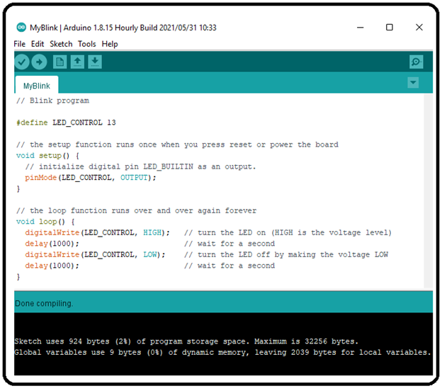
With a functioning breadboard ‘test-bed’, we can write our Simon game code, compile the code, and upload the firmware to the processor for thorough testing and debugging. Writing the code, as well as testing and debugging the code, is an ongoing process in itself. How much time will be expended is directly related to how far you want to go with it, over and beyond what is required to create a functional Simon game.
In my case, I decided that I wanted to make my hardware badge hackable. I added some code that, using the UART (Universal Asynchronous Receiver/Transmitter) connection, I could connect a TTL-USB adapter, then use a terminal program like minicom and access a shell into the code to uncover a hidden menu with hidden CTF challenges. The UART serial interface allows for two-way communication between the badge and the terminal program. For example, the terminal program can receive any data that the processor might be sending and display it in its console.
As you might guess, the amount of time you spend on software development is only limited by your imagination and the number of features you want to provide. Of course, there may be time constraints when targeting your badge for a specific conference.
Now would be a good time to consider the printed circuit development phase of the process, as fabrication lead-times can be 25 to 30 days or more. Fortunately for us, we can continue writing and tweaking the code during these long delays in the production process.
CAD Design Phase
Computer-aided design is the use of computers to aid in the creation, modification, analysis, or optimization of a design. This software is used to increase the productivity of the designer, improve the quality of design, improve communications through documentation, and to create a database for manufacturing. (Wikipedia)
There is quite a selection of CAD software available to choose from. Many are free, many are expensive, and many are somewhere in the middle. In addition, many CAD software systems are geared toward specific applications such as building/housing construction and floor-plan layouts, 3D modeling, printed circuit board design and fabrication, etc. Of course, we’re interested in PCB design software and there is an abundance of choices here as well (Altium, Altium 365, Autodesk Fusion 360, Autodesk EAGLE, KiCad EDA, Ansys RedHawk, EasyEDA, etc.). Back in the mid-80’s, I experimented with a package known as Orcad, which still exists today.
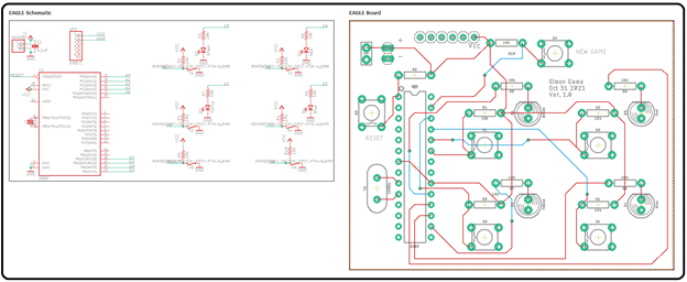
Last year, I downloaded the free version of Autodesk’s EAGLE and went to work learning their CAD design software. My first project with learning the inner workings of EAGLE was a thru-hole version (no surface mount components) of the Simon game. Although it was a slow process (learning EAGLE as I go), I successfully created the schematic, board layout, and routing. As is the case with all good CAD software, with a click of a button, I was then able to generate the Gerber files, drill hole file, BOM (build of materials) file, and Pick and Place file (picking and placing the SMT components). These files are required by the PCB fabrication company that will be building and assembling the finished PCB product.
In the case of my experimental ‘learning EAGLE’ printed circuit board, there was no assembly being done at the fabrication house. I had opted to go with thru-hole rather than surface mount components (for ease of assembly), and ordered 5 boards with no component assembly. The total cost was only $30, with a fabrication build lead-time of only 4 – 5 days. When I received the boards, I soldered the components by hand and soon verified it operated as intended.
My experience using the EAGLE software was a rewarding one, however it literally took me weeks to complete this fairly simple design. One of my biggest obstacles to overcome was learning how to traverse the vast sea of libraries in order to find the correct components for my application. I could only imagine how difficult it would have been had I gone with the low-profile surface mount device (SMD) technology approach. Additionally, learning the various EAGLE command tools also took considerable time to get through. That being said, I’m sure with more time invested, and as new projects materialize, the design process will become easier and completion times will get better.
This raises an important point worth some consideration. When the hardware badge is intended for a specific conference, and tight deadlines need to be met, I felt that it might be a better option to outsource the CAD design work to a competent professional. This was the case on my first conference hardware badge (CyMon) and the focus of this write-up. I was concerned with the amount of time it would take me to get back up to speed using EAGLE, as it had been close to a year since I had worked with it. Additionally, I wanted to go with low-profile surface mount devices on this version, and that meant searching through new libraries. To complicate things even further, we were talking about an order of 800 PCBs, which completely ruled out any manual assembly of the components.
Fortunately, a colleague (my son) recommended that I check out a website called https://fiverr.com, where professionals of many different fields offer their services and compete with others for your business. In my case, I searched for PCB designers and reached out to a few of them. In the end, I was quoted a price of $80, with 2 revisions and 2-day delivery of the Gerber, Pick and Place, and BOM files. This appeared to be the obvious way to go, considering the tight conference deadlines I was facing.
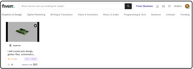
Hiring a PCB designer based in Pakistan, who I found on the FIVERR website, I had the PCB fabrication files in-hand in 2 days as promised. In order to accomplish this, I had to provide him with rough schematic (can even be hand drawn with paper and pencil). The following image illustrates what I created in Microsoft Paint and provided to my designer.
Printed Circuit Board Fabrication Phase
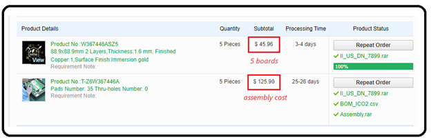
With my Gerber zip, BOM, and PnP files in-hand, it was time to reach out to my favorite (at that time) PCB manufacturer, PCBWay in China. I had used this fabrication house a year ago on my simple thru-hole CyMon board and was already familiar with their requirements and their pricing. Of course, I knew that the lead-times and pricing would be greater for this order as I was using low-profile SMD components, and they would be doing the ‘pick and place’ assembly. Unlike my former PCB order (boards only), this PCB order would be a two-step process. First, they will fabricate the PCBs (4 to 5 day lead time), and then they will assemble the components (25 to 30 day lead time). Likewise, there will be two costs involved.
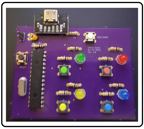
Bonus tidbit: Rather than going with a plain purple board, I discovered that I could choose from a variety of colors for my solder mask (thin lacquer-like layer of polymer that is applied to the copper traces of a printed circuit board for protection against oxidation and to prevent solder bridges). This allows me to ‘paint’ my board black and place a white silk-screen image of my choosing on the board.
Hardware Badges In-Hand — Testing Phase
So, a month later and with five prototypes in-hand, it’s time to power up a board and watch the magic! WARNING: DO NOT DO THIS!!! Unfortunately, I did that very thing, and not once, but twice! I found out the hard way that PCBWay had installed a batch of processors from Thailand that were incorrectly stamped (pin-1 designation was marked in the wrong corner of the device). Although this is a very rare condition, there have been cases where this has happened, especially with cloned knockoffs. Microchip/Atmel does not recognize the ATMega328P-UTH as a valid certified part, yet we see that part in many products, including Arduino’s Pro Micro and Pro Mini production boards.
As I stated very early in this write-up, “Active components can be severely damaged if wired incorrectly.” As the microprocessor (active component) was placed in the wrong orientation due to the incorrect pin-1 markings, applying power to the board placed Vcc voltages on the wrong pins and permanently damaged the device. Thinking this might have been a defective board out-of-the-box, I tried a second board and obtained the same results. So, at this point, I got out my multi-meter and started checking point-to-point connections for continuity. In particular, I checked for continuity between the yellow, blue, red, and green LEDs and D10, D11, D12, and D13 respectively (see schematic above). After some time, I discovered that the D10 – D13 pads were not aligned with the pin numbers according to the ATMega328P pinout. I then determined that if we lift the chip and rotate it counter-clockwise one turn, it will then be aligned correctly.
With two boards potentially damaged, that left three that might possibly be salvaged. Using a heat gun, another colleague (Rick Wisser) removed the processor(s), cleaned the land areas, and placed the chip (rotated counter-clockwise one turn). This time, when powered on, the OLED display powered on and we were good to go. With three working units, the next step was to program these boards by uploading the software for functional testing.
Valuable Lessons Learned
Always do a quick continuity check of the prototype PCB, especially with regard to the active components. Do this BEFORE POWERING UP THE BOARD for the first time! Unfortunately, we now need a second order of prototypes and we have to do the design and fabrication processes again (another 30 day wait) to ensure proper orientation going forward. After talking with my designer and attempting to understand how this rare chip orientation issue happened, I learned that there are also devices out there with various footprints (pin-1 top-left corner, pin-1 bottom-left corner, etc.). This being the case, we must always be sure to verify the correct position for pin-1 to be sure it coincides with our created board layout during the design phase. Note: As I recall, the fabricator (PCBWAY) did reach out to us via email and ask us to verify the location of pin-1 to ensure proper placement of the processor. The designer confirmed the top-left corner (which apparently was incorrect for that particular footprint).
After two shipments of prototype PCBs, and verifying that the programmed boards worked as intended, we were now ready to place a large order of 800 PCBs.
Unfortunately, this resulted in yet another valuable lesson. When choosing our board components, we must always ensure a sufficient in-stock quantity at the build house. In our case, a critical component for our board now showed as ‘out of stock’ at the build house. We now had three options: swap the component for a compatible device, supply our own parts from a third party source (such as Mouser, Digikey, etc.), or DNP (do not place) the component. In our case there were no compatible components for our part, and after checking with a number of local outlets, we soon discovered that all of the major distributors were also out-of-stock and with a back-order well into next year. Realizing this, we decided to suspend placing our order and put the project on hold for the time being.
Lead Times Can Hurt
Throughout this hardware badge project, something became very clear to me. I soon realized that at various stages of development, I found myself waiting on deliveries. I waited on delivery from my CAD designer for the BOM, Gerber, and Pick and Place files (for days at a time). Even more, I waited on my PCB fabricator (build house) in China, averaging a month to receive fully assembled parts in-hand. Additionally, there were frequent email messages from Pakistan and China requesting further information regarding questions that arose. Due to time zone differences, these would result in an additional 1 or 2 days delay.
Going forward, it became apparent that if I wanted to speed up the process, I needed to address these time consuming roadblocks. This prompted me to revisit learning the CAD software, in an effort to remove the need for outsourcing the design work. This would not only reduce costs, but would also eliminate the delays associated with corresponding with my designer in Pakistan and waiting for my files in-hand. Also, by taking control of the design process, I would be in a better position to correctly answer the many questions that might arise.
Fortunately for me, I came across a very user-friendly (and FREE!) CAD design software package called EasyEDA. Thanks to my previous experience with Eagle (now being sold as Fusion 360), I quickly came up to speed with EasyEDA. In no time at all, I had designed a half dozen ‘practice’ boards (using low profile SMT components) and verified their proper functionality. Also, related to my EasyEDA discovery, I found another PCB fabricator (JLCPCB) that was able to build and assemble my boards in less than half the time of other manufacturers. Doing my own design work meant one time consuming obstacle was now a non-issue!
Addressing the lead times associated with using the build houses in China would be a bit more challenging. It would be worth stating again, that there are actually two lead times associated with building the PCB. The first lead time is generally 3 to 5 days and involves building the bare, printed circuit board with copper routing, silk-screening, solder-masking, etc. (no components assembled). The second, and larger, lead time is typically 25 to 30 days and involves hand soldering any thru-hole components and picking and placing all SMD (surface mount devices), using specialized equipment. Obviously, there would be substantial time savings if we could do our own assembly, not to mention a substantial cost savings (assembly is typically 75% of the total PCB fabrication costs).
What is a Pick and Place Machine?
As the name implies, a Pick and Place (PNP) machine is an automated robotic machine, used to pick up and place or position SMD components on a PCB. It uses a vacuum to lift a component off of a piece of tape, rotate it to the right orientation, and precisely place it on a circuit board. This is accomplished under the control of specialized software, together with our provided PnP files. It can take some time to set up a machine to build the assembly, but once everything is up and running, it can assemble PCBs very quickly.
High-end Pick and Place machines used by the major PCB manufacturers can cost tens of thousands of dollars, while used equipment can also come with a huge price tag. Additionally, the software necessary to operate the equipment may be proprietary and could require special licensing or annual subscriptions. At the time of this writing, we are following an open source project (OpenPnP) and considering the purchase of the LumenPnP machine https://opulo.io/products/lumenpnp by Opulo. The cost is a fraction of the higher volume production machines. Shipment is scheduled for the end of the 3rd quarter this year (September 30th).
The fact that this is an open-source project is a bonus, as we will have the support of the community for future enhancements, and we will not have to be concerned about proprietary software or possible licensing issues.
We would continue to outsource the fabrication of our bare-boards (3 to 5 day turn-around and very cost effective), but using our own PnP equipment will allow us to assemble our own components and help to significantly reduce the large lead times and higher assembly costs.
Summary
Due to the constantly moving pieces (lead times, manufacturing questions, supply chain costs and availability, etc.), we need to ensure that we provide a sufficient amount of time to complete the badge on time for a targeted conference. At the time of this writing, we are still feeling the effects of the pandemic supply-chain issues. Besides availability issues, one example of this was the increase in price of the ATMega328P-AU microprocessor, which climbed from $2 to $57. Fortunately, the prices are now returning back to normal (down to $21 three months ago) and presently sitting at $4.46.
As we have seen, the longest turn-around times are PCB fabrication related. Every order of fully assembled prototypes can take a month to receive in-hand. All changes, modifications, and additions to the existing design (Gerber and Pick and Place files) will require a new set of prototypes to be generated. This results in updated files from the designer (2 to 4 days), and another 25 to 30 day lead time from the PCB fabricator (China), which adds an additional cost to our overall budget.
When taking on your hardware badge project and allowing for unforeseen issues, four to six months may appear to be a sufficient amount of time under ideal conditions. However it would always be better to get started a year in advance (whenever possible) of the targeted conference date. Fortunately, these project time allotments can be greatly reduced as we gain more experience, and by identifying and reducing the time consuming obstacles. There’s nothing more frustrating than knowing your hardware design is correct and your software works as intended, only to be delayed by out-of-your-control issues that quickly bring that target deadline ever so close.
Hopefully, knowing in advance of the potential obstacles and taking the necessary steps to reduce or eliminate them, we can greatly enhance our chances of successfully delivering our finished product ahead of schedule.
Ready to learn more?
Level up your skills with affordable classes from Antisyphon!
Available live/virtual and on-demand