JTAG – Micro-Controller Debugging

Being an embedded firmware engineer for most of my career, I quickly became fascinated when I learned about reverse engineering firmware using JTAG. I decided to take on this project as an opportunity to learn more about this somewhat obscure and often overlooked attack vector.
excerpt from: https://en.wikipedia.org/wiki/JTAG
JTAG (named after the Joint Test Action Group which codified it) is an industry-standard for verifying designs and testing printed circuit boards after manufacture. JTAG implements standards for on-chip instrumentation in electronic design automation (EDA) as a complementary tool to digital simulation. It specifies the use of a dedicated debug port implementing a serial communication interface for low-overhead access without requiring direct external access to the system address and data buses. The interface connects to an on-chip Test Access Port (TAP) that implements a stateful protocol to access a set of test registers that present chip logic levels and device capabilities of various parts. The Joint Test Action Group formed in 1985 to develop a method of verifying designs and testing printed circuit boards after manufacture. In 1990 the Institute of Electrical and Electronics Engineers codified the results of the effort in IEEE Standard 1149.1-1990, entitled Standard Test Access Port and Boundary-Scan Architecture.
JTAG is an industry-standard Test Access Port for debugging and running diagnostics of integrated circuits after a PCB has been assembled. Originally providing manufacturers with a simplified way to test a circuit board design, it’s even more relevant now that devices are using a Ball Grid Array (BGA) making it difficult to test due to the reduced size. Additionally, an exposed interface creates the means for engineers to assess the signals without directly interfacing using physical connections to circuits.
After reviewing a variety of JTAG related videos, I discovered a number of positive benefits in gaining access to the target device, especially the ability to read and write to these devices. The possibilities seemed endless.
In an effort to get started, I located a Linksys BEFSR41 ver2 router at a local garage sale, and it was ‘game on’ to begin experimenting with a few of the many JTAG hardware and software tools. I was determined to duplicate the efforts and accomplishments of some of those videos that I had witnessed.
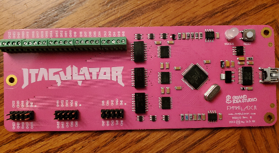
After much research, I decided to purchase the JTAGulator board from Parallax, and a couple of popular serial interface boards, DangerousPrototypes Bus Pirate and Bus Blaster, as well as the Attify Badge.
I started with the JTAGulator, an open-source hardware tool designed by Joe Grand to not only locate, but also identify the JTAG pins on the target board, which in turn, provides the ability to find on-chip debugging (OCD) interfaces. Also featured on this tool is the ability to locate and identify UART pins.
Locate and identify the JTAG pins on the target board
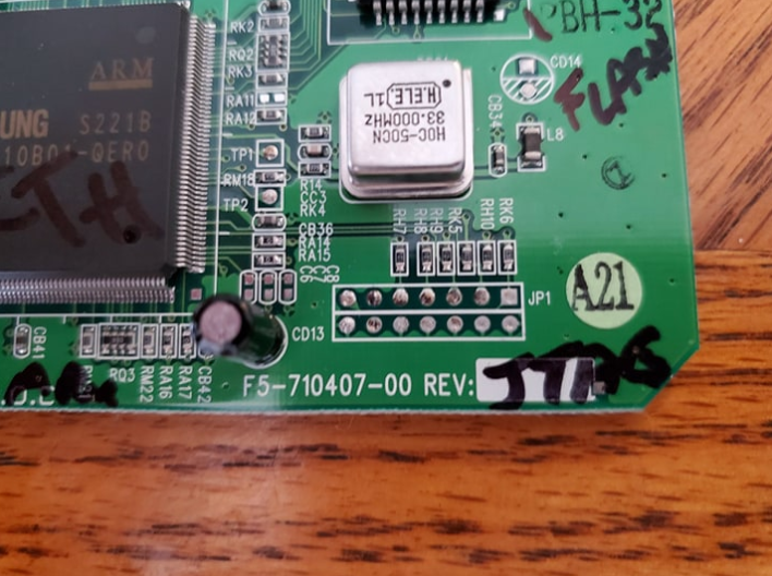
Before getting started, I first located and printed datasheets for the target board, the Linksys BEFSR41 ver2 router.
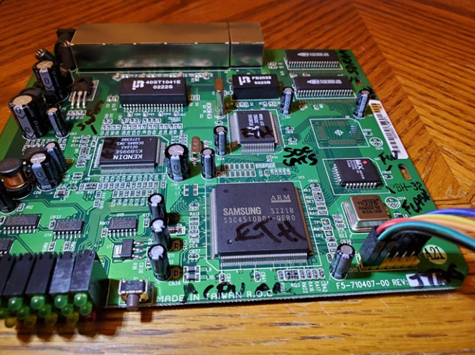
I quickly found the following devices on board:
CPU: Samsung S3C4510001 ARM7TDI 50Mhz
Flash memory: MX 29F040QC-90 5 volt CMOS ( 512Kbit x 8 ) 0.5 Mbyte
SDRAM memory: SI IC41C16256-35K x2 512Kbyte – 256K x 16 dynamic RAM
Ethernet controllers: RealTek RTL8019AS ISA Full-Duplex Controller
KENDIN KS8995E 5-port 10/100 Integrated Switch
Based upon information that I acquired watching instructional videos for the JTAGulator board (by its author Joe Grand), I determined what I thought might be a JTAG TAP (test access point) at JP-1.
Joe Grand’s JTAGulator video: https://www.youtube.com/watch?v=GgMOBhmEJXA
Identify the JTAG pins
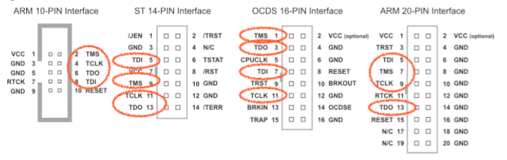
Often you’ll find TMS, TCK, TDI, TDO, etc inscribed on your PCB, so you know you’re dealing with a device that supports JTAG, but it gets more difficult when the pins aren’t labeled and you need to rely on third-party documentation.
Of course, it is also possible that your board has a JTAG header instead of mere pins/contacts. JTAG access points are often intentionally hidden by the board designers, and in most cases lack headers or board markings. You might also get the datasheet on the on-board micro-controller. Sometimes, the pins are marked with JTAG references and the PCB traces might lead out to an access point.
For example:
On my target board, JP-1 is a header-less 2 x 7 row of feed-thru pin sockets.
Finally, I needed to locate ground on the target device and jumper it to a GND pin on the JTAGulator board. NOTE: The JTAGulator and the target device MUST share a common ground point (to ensure proper reference voltages and reliable readings) before continuing with any testing.
Also, using a desoldering tool (solder sucker), I cleared the solder from the JP-1 pin sockets and soldered in (2) 7 pin male headers to facilitate hooking up jumper wires for my debugging.
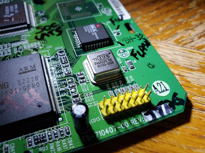
Using a multimeter, I determined that pins 2, 4, 6, 8, 10, 12, and 14 were all tied to circuit-ground. This left 8 (unknown) pins, of which 5 could be the 4 required (and 1 optional) JTAG pins:
- TDI Test data in
- TDO Test data out
- TMS Test mode select
- TCK Test clock
- TRST Test reset (optional)
Using channels 0 through 7 on the JTAGulator board, I connected jumper wires to the 8 (unknown) pins on the target device (order of connection was not relevant). Note: pin-14 is the green (GND) jumper wire.
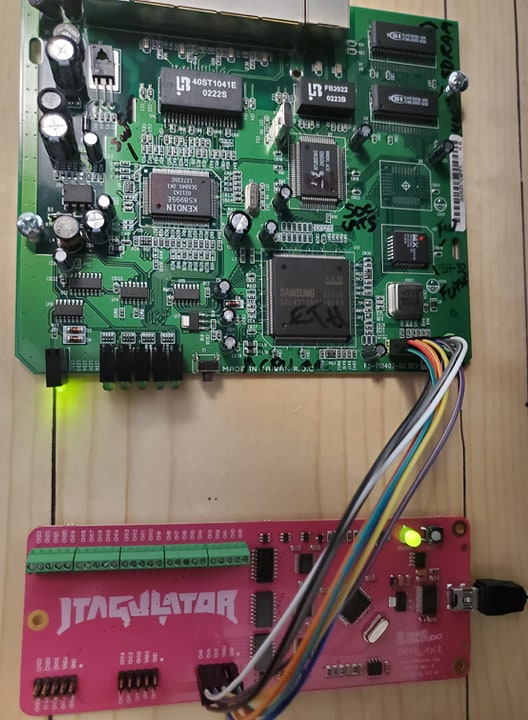
At this point, I powered the target device (using the manufacturer provided 9VDC adapter) and then powered the JTAGulator board via the mini-USB cable to my Linux desktop.
In a command shell on my Linux machine, I located the serial port of the JTAGulator and established a serial connection to it using picocom, a minimal dumb-terminal emulation program that is great for accessing a serial port based Linux console.
Installing picocom:
On Ubuntu, you can simply:
sudo apt-get install picocomExcerpt from the QuickStart instructions: https://www.parallax.com/sites/default/files/downloads/32115-JTAGulator-Product-Brief-1.1.pdf
The JTAGulator is powered from the host computer’s USB port and uses an industry-standard FTDI FT232RL device to provide the USB connectivity (drivers available from www.ftdichip.com/Drivers/VCP.htm.) The device will appear as a Virtual COM port and will have a COM port number automatically assigned to it. All communication is 115200 bps, 8 data bits, no parity, 1 stop bit. Use a terminal program (for example, HyperTerminal, PuTTY, CoolTerm, picocom, or screen) to communicate with the JTAGulator.
$dmesg | grep tty(determine serial device port)
$sudo picocom -b 115200 -r -l /dev/ttyUSB0( -b = baudrate and -r = no reset and -l = no lock )
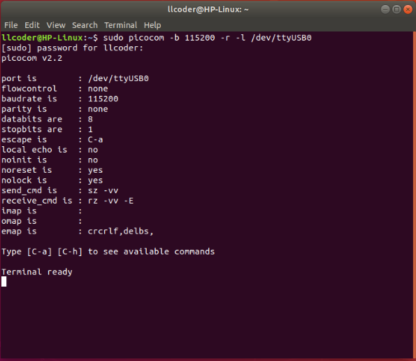
Clicking [ENTER] gets me the ‘:’ JTAGulator command prompt
: H (prints available commands)
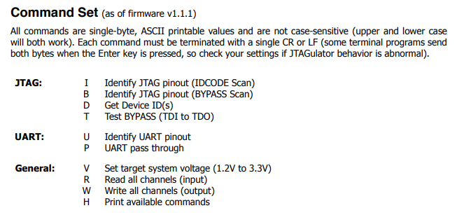
Before proceeding any further, I needed to determine the system voltage of the target device. This was done using a multimeter set up for DC voltage measurements and checking various points around the target board (including the header that I soldered in). It was determined the system voltage was 3.3 volts.
: V Set target system voltage (1.2V to 3.3V)
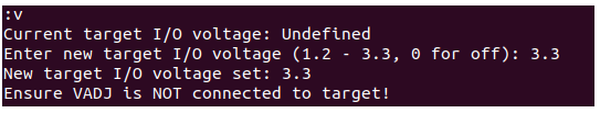
Before executing the Identify JTAG pinout (BYPASS Scan), I performed an Identify JTAG pinout (IDCODE Scan)
Executing the ID code scan is considerably faster than the Bypass scan (TDI is not required, resulting in fewer scan permutations), although the ID scan only finds 3 of the required 4 JTAG pins.
: I Identify JTAG pinout (IDCODE scan)
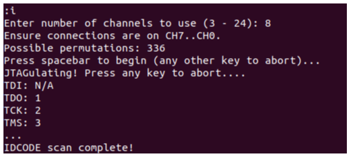
Executing the Get Device ID(s) command provides …
: D Get Device ID(s)
Executing the Identify JTAG pinout (BYPASS scan) command provides us with the 4 required JTAG pins (and optional TRST pin) assignments.
: B Identify JTAG pinout (BYPASS scan)
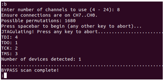
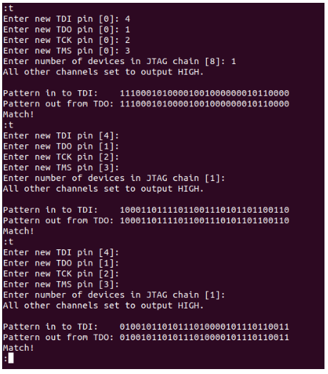
Executing the Test BYPASS (TDI TDO) command verifies that the 32 bits of random data sent out on TDI to the target device, is correctly returned on TDO back to the JTAGulator
: T Test BYPASS (TDI TDO)
Summary
Using the JTAGulator when attempting to identify suspected JTAG pins, is always going to be an invaluable tool and highly recommended. Together with knowing the JTAG pinout, connecting a JTAG compatible USB adapter and some good debug tools (OpenOCD, GDB, binwalk, etc), you should be successful in communicating with your hardware target.
In conclusion, it’s safe to say, that vendors may soon realize the importance of hiding these TAPs to protect their proprietary interests. These TAPs have been around for a long time, and I don’t see them going away any time soon, as they do provide importance to the manufacturing cycle. Using the methods mentioned above, along with acquiring the appropriate SoC (System on a Chip) datasheets, could help you locate the more obscured TAPs. Many times, just looking near the chip itself can provide clues. Other times, the TAPs may be hidden under the SoC in question, requiring chip removal. Following traces, difficult as it may be, can also guide you to potential test points.
Ready to learn more?
Level up your skills with affordable classes from Antisyphon!
Available live/virtual and on-demand